A conducted emissions test failure does not always mean the PCB needs to be redesigned. In many cases, conducted EMI can be reduced through filter upgrades, grounding improvements, shielding, cable treatment, and system-level adjustments while keeping the existing PCB layout unchanged.
Although PCB redesign can address fundamental EMI sources such as ground-plane structure, trace routing, and return-path impedance, it also increases engineering time, validation workload, and production cost. For hardware that is already finalized or approaching production, engineers therefore need practical conducted EMI mitigation strategies that can be implemented without a complete board revision.
Available solutions are often more effective than many engineers anticipate. While PCB architectural modifications (ground plane design, impedance control, trace routing) cannot be easily altered once the board is finalized, component upgrades, optimized installation practices and system-level adjustments frequently deliver enough noise attenuation to meet EMC requirements — in many cases, with zero PCB redesign.
This article explains how to troubleshoot and reduce conducted EMI through component, installation, grounding, shielding, and external filtering improvements before deciding whether PCB redesign is necessary.
Filter Component Upgrades Within Existing Constraints
One of the first areas to evaluate is whether the existing EMI filter can be upgraded within the available mechanical and electrical constraints. If your PCB already has allocated space for a filter with standard mounting (solder pads or threaded terminals), higher-performance alternative filters with mechanically compatible packages are widely available.
Many filter manufacturers offer multiple performance tiers in the same package. A basic shunt capacitor approach might be replaced with a common mode choke, a Pi topology might be upgraded to a higher-capacitance version, or a standard L-C filter might be upgraded to a multi-section design. Each of these changes can provide 5–20 dB or more improvement in attenuation at the frequencies you need to suppress.
Before selecting a replacement filter, confirm three critical requirements:
- The mechanical package fits the existing PCB footprint;
- The mounting method (threaded, through-hole solder, SMD) matches the board design;
- Electrical attenuation performance is improved across your target troublesome frequency range.
Most component manufacturers can quickly suggest compatible alternatives when you share the existing part number and your required improvement in noise suppression.
Installation Quality: Frequently the Fastest Performance Improvement
Filter performance is heavily influenced by installation quality. Numerous designs fail to realise the full attenuation capability of selected filters simply due to suboptimal mounting practices. Optimising installation often incurs zero extra cost and can recover 3–10 dB or more of lost noise suppression.
For solder-in filters: Verify that solder joints are continuous and void-free. Inspect by X-ray or microscopy if possible. A cold solder joint or internal void increases contact resistance, which damps the filter’s response and reduces effectiveness. Re-soldering or reworking a poor joint can immediately improve performance.
For threaded (bolt-in) filters: Thoroughly clean the mating mounting surface. Remove paint, oxidation layers and anodised coatings at the interface between filter housing and chassis. Fasten according to the torque specification provided by the manufacturer. Insufficient torque reduces contact pressure and effective contact area, increasing interfacial resistance. Excessive torque risks permanent mechanical damage to the filter component.
Both of these improvements require no PCB changes and no new components. They should be among the first things to verify when facing an EMI issue.
Grounding and Bonding Improvements
Common mode noise performance is extremely sensitive to grounding quality. Optimizing ground and shield bonding frequently delivers significant EMI suppression with relatively low cost.
Chassis-to-PCB grounding: Ensure robust electrical connection between the PCB and chassis at multiple locations, not only near the filter. If physically accessible, install external bonding straps without altering the PCB layout. These straps establish low-impedance return paths for common-mode currents and limit noise coupling into circuits.
Filter ground connection: Ideally, the filter ground path to PCB or chassis should be short and direct. Multiple parallel vias (4–8 for high-frequency designs) minimize return-path inductance and boost high-frequency filtering performance. Note that adding vias constitutes a PCB layout modification; this remedy is only viable before board production and cannot be implemented on finished PCBs.
Ground plane discontinuities: Voids, splits and cutouts in the ground plane near the filter force noise currents to take longer detoured paths and raise stray inductance. Remedying ground-plane gaps requires PCB redesign, so this factor should be addressed in early hardware revisions rather than used as a late-stage fix for finished hardware.
Shielding and Cable Management
External shielding and cable ferrite treatment deliver cost-effective EMI reduction and require no PCB redesign.
Ferrite beads or sleeves: Installing ferrite sleeves over power or signal cables near the enclosure entry point involves no PCB changes and carries minimal cost. Ferrite components mainly suppress high-frequency common-mode noise. Their attenuation depends on operating frequency, cable impedance, and winding turns; looping cables through the ferrite core can boost performance. Typical attenuation gains of 5–15 dB can be obtained on target noise frequencies. This fast, low-cost countermeasure should be prioritised during early troubleshooting.
Cable shielding: Unshielded cables act as efficient radiating antennas. Upgrading to shielded cables reduces both radiated emission and noise coupling. Effective shielding relies on proper termination: use 360° shield bonding at the enclosure entry. Short pigtail ground leads add parasitic inductance and severely limit shielding effectiveness at high frequencies.
Enclosure modification: Minor mechanical adjustments can improve EMC performance without PCB revisions. Common measures include sealing unused panel apertures, establishing robust grounding for internal shielding, and separating noisy cables from sensitive circuits. These low-cost adjustments can be implemented during production assembly or field retrofits.
Input Filtering Additions
When conducted EMI invades the equipment via power or signal cables, input-side filtering intercepts noise before it couples into internal circuits.
Power entry filtering: If mechanical space permits, mounting an EMI filter at the AC or DC power inlet can deliver 20–40 dB or higher attenuation for conducted power-line noise. This stops grid-borne noise from propagating to sensitive internal circuitry. Note that attenuation values are specified under standard 50 Ω test conditions; actual performance depends on system impedance matching. Many power entry filters share standard connector form factors and only require minor mechanical adjustments instead of full PCB redesign.
Signal line filtering: For signal cables penetrating the enclosure boundary, install filtering at the entry point — options include ferrite beads, series inductors, or integrated filter networks. This blocks conducted external noise at the shield boundary, instead of attempting noise suppression deep inside the chassis. Engineers must balance filtering performance with signal integrity; filter components may distort high-speed signals if improperly selected.
Measurement and Validation
Measurements are mandatory before and after every modification. Without comparative testing, engineering resources and budget are easily wasted on adjustments that deliver negligible EMI reduction.
Establish a baseline: Capture the conducted emissions profile of the original design. Pinpoint the frequency bands failing compliance and distinguish common-mode and differential-mode noise where possible. Calculate the required attenuation margin to pass relevant EMC standards with sufficient safety headroom.
Measure impact of each change: Implement modifications one at a time, or in logically related groups, and re-test after each adjustment. This method clearly separates effective countermeasures from ineffective ones. Remedies perform differently depending on system noise characteristics; a solution that works for one frequency spike may barely affect others.
Focus effort on high-impact changes: Prioritize adjustments delivering the greatest attenuation gain based on test results. For example, upgrading an input filter may deliver 12 dB improvement, chassis grounding optimization around 6 dB, and cable ferrites roughly 5 dB. Note that decibel improvements cannot simply be summed mathematically due to noise phase and impedance shifts. In many cases, combining multiple moderate improvements can reach the required attenuation target without PCB redesign.
When Remediation Will Not Be Sufficient
Not all EMI problems can be solved without redesign. Recognize these warning signs:
- Dominant EMI source is PCB layout:If the problem originates from high-impedance ground returns or poor trace routing, component changes will have limited effectiveness.
- Multiple failures across frequency ranges:If EMI failures span low, mid, and high frequencies, a single filter upgrade will not address all of them.
- No space for filter upgrades:If the PCB layout has no room for a larger or more complex filter, remediation options are limited.
- Marginal compliance even with upgrades:If after implementing practical remediation (filter upgrade + grounding optimization + shielding), the margin is still inadequate, redesign is likely necessary.
Measure to verify what is actually limiting performance. This helps distinguish between problems that can be remediated and problems that require redesign.
Frequently Asked Questions
Q: Can I improve EMI just by changing the filter component? Yes, often. Filter performance spans a range depending on the specific component. If your PCB accommodates a higher-performance filter in a compatible package, upgrading can provide 5–20 dB or more improvement. Verify that the new component is mechanically and electrically compatible before ordering.
Q: What is the easiest, lowest-cost EMI improvement? Start with installation quality: verify solder joints, remove oxide/corrosion from ground surfaces, and ensure correct torque on threaded filters. This costs almost nothing and often recovers 3–10 dB. Second, evaluate ferrite beads on power or signal cables — also very inexpensive. Measure the impact of each change to guide further investment.
Q: How much improvement should I expect from ferrite beads? Ferrite beads typically provide 5–15 dB improvement depending on the frequency range and cable impedance. They’re inexpensive and require no PCB changes, so they should be one of the first things to try. Measure the impact to confirm effectiveness for your specific problem.
Next Steps
Reducing conducted EMI without PCB redesign usually requires a combination of targeted troubleshooting, filter evaluation, grounding optimisation and installation improvements rather than a single universal fix. Engineers should first identify the failing frequency range and noise mode, then evaluate each mitigation measure through comparative conducted emissions testing.
When selecting or upgrading EMI filtering components, insertion loss should be considered together with source and load impedance, grounding quality, mounting configuration, current and voltage requirements, and the available mechanical space. A filter that performs well under standard laboratory conditions may behave differently once installed in the actual system.
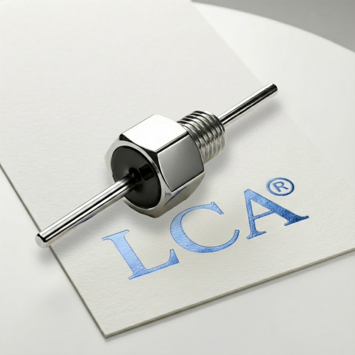
Based on LCA’s experience supporting EMC-critical applications, component selection should therefore be evaluated together with the complete installation environment. For projects requiring alternative feedthrough capacitors, Pi filters, LC filters or customized EMI filtering configurations, LCA can support engineers in evaluating suitable solutions based on the electrical, mechanical and attenuation requirements of the application.
Technical guidance in this article reflects general EMI remediation principles. Actual performance depends on system architecture, operating conditions, noise frequency and installation environment, and all modifications should be validated through appropriate EMC testing.
Technical guidance in this article reflects general EMI remediation principles. Actual effectiveness of specific changes depends on the product design, frequency of the EMI problem, and the actual circuit conditions. Always measure before and after any changes to verify effectiveness. Some products may require full PCB redesign if component-level remediation proves insufficient.