An EMI filter’s attenuation performance measured inside standardized laboratory test fixtures often deviates drastically from its real-circuit performance after physical installation. The identical filter part that meets published insertion loss specs in ideal test setups frequently loses several decibels of high-frequency noise suppression in end equipment. This performance gap rarely stems from defects within the filter component itself; it is driven by the impedance and integrity of the ground path that shunts interference to PCB ground or metal chassis.
This article explains why grounding quality matters as much as component selection, what grounding practices preserve filter performance, and how to verify that your EMI filter installation will deliver the insertion loss you designed for.
Why Filter Performance Depends on Grounding Quality
The Ideal Ground Reference for Datasheet Testing
All published insertion loss figures of EMI filters are measured inside standardized test fixtures under fixed ideal conditions: a dedicated nearby reference ground plane, ultra-short direct bonding traces, and low-parasitic-inductance noise return paths. Within this controlled test setup, the filter’s shunt capacitors can deliver their full designed noise-shunting impedance to ground.
The Reality of Actual Installations
In physical PCB layouts or chassis-mounted filter assemblies, every ground return path carries unavoidable parasitic inductance, originating from four key sources:
Trace length: If the ground connection is made through a PCB trace rather than a direct connection, the trace acts as an inductor. A 1 cm trace at 1 GHz can have impedance of several ohms — enough to significantly degrade filter performance.
Via inductance: Even a short via connecting the filter to a ground plane has parasitic inductance on the order of 0.5–1 nanohenry. At frequencies above 100 MHz, this inductance becomes significant relative to the capacitive impedance of the filter.
Ground plane discontinuities: If the ground plane has a void or trace crossing near the filter location, current must detour around it, taking a longer path and introducing additional inductance.
Poor contact at connection points: Solder joints with voids, oxidized surfaces, or paint at a chassis ground connection all increase contact resistance. This resistance damps the filter’s resonance and reduces insertion loss.
All impedance within the ground return path acts in parallel with the filter’s shunt capacitors, raising the effective ground impedance and lowering overall insertion loss. This performance degradation is most severe above tens of MHz, where parasitic inductance becomes the dominant reactive factor.
Grounding Strategies & Corresponding Applicable Scenarios
No single grounding method delivers optimal performance across the full frequency spectrum. The proper grounding layout must be selected based on the target noise frequency band to be suppressed.
Single-Point Grounding at Low Frequencies
For low-frequency operation (generally below 1 MHz), resistive impedance dominates ground return paths while inductive reactance remains negligible. One unified ground terminal can carry all return current with sufficiently low impedance. Single-point grounding is recommended for such low-frequency systems, as multiple ground taps will create ground loops and induce extra mains-frequency or harmonic noise.
Multi-Point Grounding at High Frequencies
At high frequencies (typically above several MHz), wavelengths become comparable to the physical size of the system. Inductance dominates the ground path impedance. Multiple ground connections at different locations provide parallel return paths, reducing the total return path inductance. Multi-point grounding is necessary to achieve the specified insertion loss at these frequencies.
Hybrid Approaches in Practice
Most industrial equipment needs noise attenuation across an ultra-wide spectrum: low-frequency power-line conducted interference plus high-frequency RF coupling. Hybrid grounding designs are widely adopted to balance both demands: one main single ground point establishes a stable DC reference for control and analog circuits, while supplementary distributed ground vias or mounting contacts are added exclusively to minimize inductance for high-frequency noise return currents.
PCB-Level Grounding Implementation
For PCB-integrated EMI filters, grounding quality depends on several interconnected design decisions.
| Grounding approach | Typical performance impact | Frequency range | Comments |
| Single via (1.0 mm diameter) | Adequate to ~100 MHz | DC to 100 MHz | Simple but limits high-freq performance |
| Multiple vias (4–8, 1.0 mm) | Good to >1 GHz | DC to GHz | Standard practice for RF applications |
| Via stitching (continuous vias) | Excellent >1 GHz | DC to GHz | Best practice for very high frequency |
| Long ground trace (>1 cm) | Significant degradation above 100 MHz | Limited above 50 MHz | Introduces inductance; avoid |
| Direct ground plane contact (no via) | Excellent if plane is adjacent | DC to GHz | Best if plane is on adjacent layer |
Via Placement and Quantity
A single through via introduces roughly 0.5–1 nH of parasitic inductance. At 100 MHz, this inductance creates 0.3–0.6 Ω of reactance — a critical impedance when matched against low-impedance high-frequency shunt capacitors. For circuits operating above 100 MHz, deploy 4–8 parallel vias to cut total equivalent ground inductance. Wider vias (12 mil diameter or bigger) deliver lower inductance than tiny vias; fewer large vias can achieve the same low-impedance effect as multiple small vias.
Ground Plane Continuity and Location
The vertical distance between the EMI filter and ground plane, plus ground copper integrity, directly determine filtering performance. Laying a solid ground plane on the layer directly below the filter minimizes noise return loop length. Continuous unbroken copper around the filter avoids detoured current paths caused by cutouts or slots. Split ground planes, signal traces crossing the ground area, or signal routing beneath filter pads all extend the ground return path and raise parasitic inductance.
Layer Stackup Considerations
For multilayer PCBs, the layer assigned to the filter strongly impacts grounding quality. Mounting filters on a layer directly adjacent to an uninterrupted ground plane outperforms placing components on outer layers, where noise must travel longer vertical paths to reach ground copper.
Chassis-Mount Filter Grounding
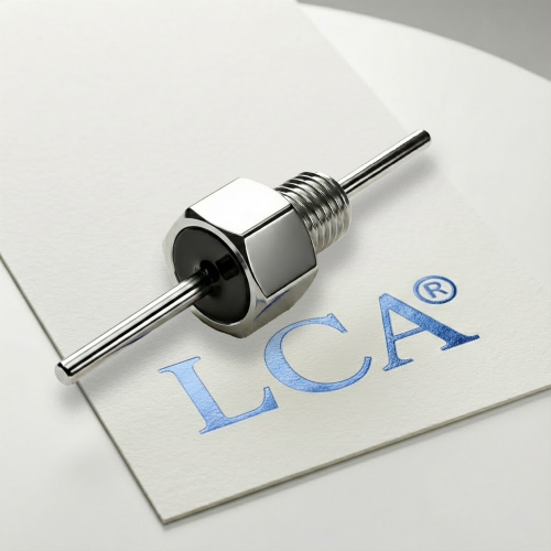
Filters mounted through metal shielding panels, including solder-in and threaded feedthrough types, rely on physical metal contact between the filter’s conductive housing and chassis to establish low-impedance grounding.
Solder-In Filter Installation
A solder-in feedthrough filter’s ground bond depends on the quality and size of the solder joint connecting the filter body to the chassis or PCB. A cold solder joint, a void in the solder, or insufficient solder volume reduces the contact area and increases contact resistance. Increased resistance damps the filter’s resonance, reducing insertion loss.
Solder joint quality should be verified by X-ray or microscopy during production. Visual inspection is not sufficient to detect internal voids.
Threaded Filter Installation
A threaded (bolt-in) filter depends on the contact area between the filter body and the chassis at the mounting interface, and on the contact pressure created by torque. Paint, anodizing, oxidation, or other surface contamination at the contact surface increases contact resistance and degrades performance.
The installation workflow must define three mandatory requirements:
Surface preparation: Remove paint and oxide within the contact area (typically 1–2 cm radius around each mounting location) to ensure clean metal-to-metal contact.
Torque value: Apply the specified torque to create adequate contact pressure. Under- torquing reduces contact area and increases resistance.
Re-verification: After thermal cycling or environmental stress, re-torque or verify contact integrity. Thermal cycling can degrade solder joints; vibration can work threaded filters loose.
Common Grounding Errors, Performance Symptoms & Corrective Actions
| Mistake | Symptom | Typical frequency impact | Correction |
| Single via for high-frequency filter | Insertion loss 50% lower at 1 GHz | Above 100 MHz | Add multiple vias (4–8) in parallel |
| Long ground trace | Performance degrades with frequency | Increases above 50 MHz | Shorten trace or use direct via to plane |
| Ground plane void or discontinuity | Localized performance loss | Especially >500 MHz | Route traces to avoid voids |
| Paint on threaded filter ground | Loss of 2–5 dB at high frequencies | Above 100 MHz | Remove paint; verify by measurement |
| Poor solder joint (solder-in) | Inconsistent performance | Primarily above 100 MHz | Verify by X-ray; rework if needed |
| Insufficient torque on threaded mount | Unpredictable performance variation | Entire frequency range | Re-torque; verify contact resistance |
Frequency-Dependent Performance: Why Grounding Matters More at High Frequencies
At low frequencies (below 1 MHz), parasitic inductance has minimal impedance, so grounding deficiencies have little effect. The filter’s capacitive shunt impedance dominates, and the filter performs close to specification even with suboptimal grounding.
At high frequencies (above 100 MHz), the situation reverses. Parasitic inductance in the ground path creates significant impedance, which shunts noise current away from the capacitor and reduces the filter’s effectiveness. A filter that meets specification at 1 MHz may provide only half the specified attenuation at 1 GHz if the ground path is not optimized.
For broadband EMI filters that must suppress both low and high frequencies, this creates a design challenge: low-frequency performance requires good DC conductivity (short path, continuous plane); high-frequency performance requires low inductance (multiple vias, direct plane contact). The solution is typically a hybrid approach that satisfies both requirements.
Troubleshooting Guide for Underperforming EMI Filters
If a filter achieves rated attenuation on laboratory test fixtures but delivers poor noise suppression after assembly, defective grounding is the top root cause. Follow this standardized troubleshooting workflow:
- Compare bench performance to circuit performance.Measure insertion loss on the installed filter using a network analyzer. Compare to the component datasheet curve.
- Identify the frequency range where degradation occurs.Degradation above 100 MHz typically points to ground path inductance. Degradation across all frequencies suggests contact resistance issues.
- Check for common grounding deficiencies.Review the ground path: Is it via or trace? Single via or multiple? Is the ground plane continuous? Is the plane adjacent to the filter or distant?
- Verify ground bond quality.For threaded filters, check for paint or oxide on the mounting surface. For solder-in filters, verify by X-ray.
- Measure ground path resistance.Use a low-resistance ohmmeter to measure DC resistance of the ground connection. High resistance (>0.1 ohms for a good connection) indicates contact or solder joint problems.
- Execute targeted improvements.Add parallel ground vias, shorten ground traces, rework defective solder joints, or clean bare-metal mounting surfaces according to troubleshooting findings.
Summary: Grounding Checklist
Before finalizing your EMI filter installation:
- Ground connection is direct and short (not a long trace)
- Multiple vias (4–8) used for high-frequency applications
- Ground plane is continuous near the filter location
- Ground plane is on an adjacent layer to the filter if possible
- For solder-in filters: solder joint quality verified by X-ray or microscopy
- For threaded filters: surface preparation performed (paint/oxide removed)
- For threaded filters: correct torque applied and documented
- Insertion loss measured on installed filter and compared to datasheet
- DC resistance of ground connection verified by measurement
- Grounding plan accounts for both low-frequency and high-frequency requirements
Frequently Asked Questions
Q: How many vias do I need for my EMI filter? This depends on the frequency and the via diameter. As a guideline, use at least 4 vias (1.0 mm diameter) for applications above 100 MHz, and 8 or more for very high-frequency applications (above 1 GHz). Verify your configuration by simulation or measurement before committing to layout.
Q: Does my EMI filter need to be mounted directly on a ground plane? Not necessarily — single-point grounding via a trace works for low-frequency applications. For high-frequency performance (above 100 MHz), place the filter on a layer adjacent to a solid ground plane or use multiple vias to achieve low-inductance connection. The closer and more direct the ground connection, the better the high-frequency performance.
Q: Can I use a single long trace for grounding instead of multiple vias? Not for high-frequency filtering. A long trace acts as an inductor, reducing insertion loss at high frequencies. For high-frequency performance, use direct vias or adjacent plane connection.
Q: Does thermal cycling affect EMI filter grounding? Yes. Repeated thermal cycling can create micro-voids in solder joints, increasing resistance. Grounding continuity should be re-verified after environmental stress testing.
Next Steps
Grounding is part of the EMI filter circuit and should be considered during component selection, PCB layout and mechanical installation. A short and low-impedance return path generally supports better high-frequency attenuation.
If you are designing an EMI filter installation or troubleshooting one that underperforms, start with the grounding checklist above. For detailed guidance specific to your application, contact LCA’s application engineering team for consultation. LCA provides solder-in, threaded and customized feedthrough filter configurations for different installation structures. Application and mounting requirements can be reviewed together with the electrical specifications before final selection.
Technical guidance in this article is based on general PCB grounding and EMI installation principles. All specific values for via inductance, contact resistance, and insertion loss degradation are approximate and depend on detailed circuit parameters. Actual performance should be verified by simulation or measurement with your specific component values, frequencies, and circuit geometry before committing to production.